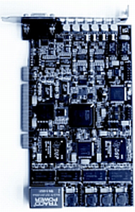
PCDSP6 DSP Board
Relcom's PCDSP6 DSP Board is a special DSP board for very complex signal porcessing application with versatile, 100% user defined resource allocation capability. The board has universal structure for wide area of high-speed complex signal processing applications. PCDSP6 is an ideal tool for high-speed (FPGA), and lower speed but more complex (DSP) signal processing applications. The card has complete signal processing capability from 70MHz IF signal to multichannel baseband digital demodulation.
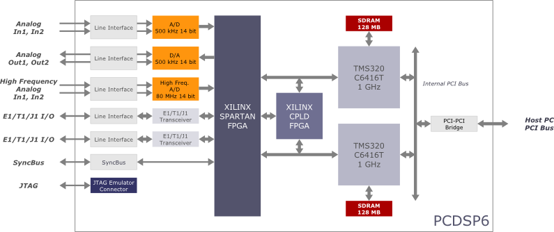
Block Diagram

Features
- Universal structure for wide area of high-speed, complex signal processing applications
- 100% user defined resource allocation capability to fit with the application need
- Ideal tool for high-speed (FPGA), and lower speed but complex (DSP) signal processing applications
- Complete signal processing capability from 70MHz IF signal to multichannel baseband digital demodulation
- High resolution DDS based sampling signal generator
- LVDS clock/sync bus for multiboard synchronization
- Two channel DAQ quality analog input and output section with programmable antialiasing filters
- Complete two-channel E1/T1/J1 receive/transmit processing capability from
- Two highest speed DSPs of the world
- SPARTANIII FPGA, which is freely programmable for the user
DSP part
- Two TMS320C6416 Digital Signal Processors
- Highest speed DSP of the world - 1GHz
- 128 Mbyte 64 bit wide SDRAM for both processors
- Local PCI bus for internal data transfer
- Very fast two port memory between DSPs
- All DSP resources can be accessed from the PCI bus
- Configurable interrupt system allowing high level flexibility
FPGA part
- 1.5 Million gate FPGA
- Fully user programmable from host PC
- Digital Down Converter core, FIFO core, two-port memory core, etc. are implemented
E1/T1/J1 input/output part
- 2 independent framers with E1/T1/J1 line interface and framer units
- E1/T1/J1 interfaces can be assigned to DSPs freely
- Signal processing capability of E1/T1/J1 signals in the FPGA also
Low frequency analog input/output part
- Two input channels with programmable gain and programmable cutoff frequency low pass filters
- Nonvolatile digital potmeters for gain and offset adjust
- 16 bit A/D converters with 500 kHz maximum sampling rate
- Versatile sampling signal sources containing external sampling source signal capability
- Two-channel 14 bit D/A converters with 500 kHz maximum update rate with programmable low pass filters
High frequency analog input part
- Two channel 14 bit 80MHz sampling rate A/D converter with simultaneous sampling capability on channels
- High resolution DDS based sampling clock generator
- LVDS clock bus for multiboard synchronous operation
Application Notes
Soon...
Documents & Drivers
-
PCDSP6 Driver and Monitor Program —
 Download...
-
PCDSP6 Software Support —
 Download...
-
XP/Vista Driver —
 Please contact to Relcom...
-
Linux Driver —
 Please contact to Relcom...

© 2009 Relcom, Ltd.


